


Your product. Your specifications. The possibilities are endless.
For more applications of graphene heating film, please free to contact with PMA team.

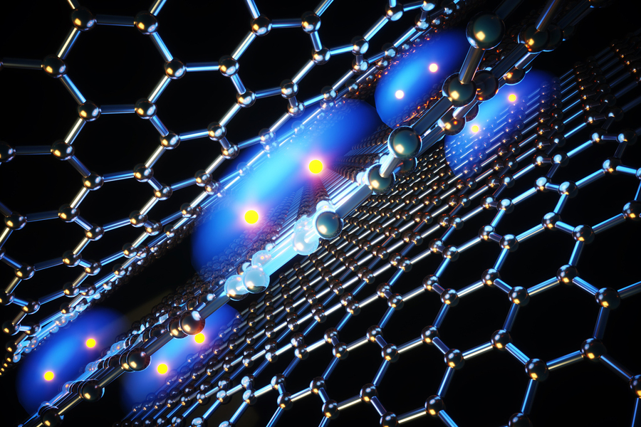
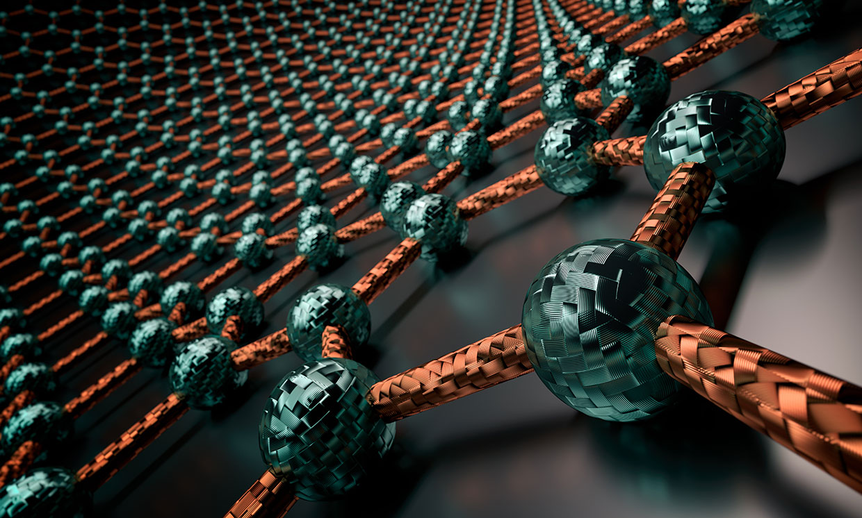
Structure of graphite and its intercalation compounds
In 1859 Benjamin Brodie noted the highly lamellar structure of thermally reduced graphite oxide.
In
1916, Peter Debije and P. Scherrer determined the structure of graphite
by powder X-ray diffraction. The structure was studied in more detail
by V. Kohlschütter and P. Haenni in 1918, who also described the
properties of graphite oxide paper. Its structure was determined from
single-crystal diffraction in 1924.
The
theory of graphene was first explored by P. R. Wallace in 1947 as a
starting point for understanding the electronic properties of 3D
graphite. The emergent massless Dirac equation was first pointed out in
1984 separately by Gordon Walter Semenoff, and by David P. DiVincenzo
and Eugene J. Mele. Semenoff emphasized the occurrence in a magnetic
field of an electronic Landau level precisely at the Dirac point. This
level is responsible for the anomalous integer quantum Hall effect.
Observations of thin graphite layers and related structures
Transmission
electron microscopy (TEM) images of thin graphite samples consisting of
a few graphene layers were published by G. Ruess and F. Vogt in 1948.
Eventually, single layers were also observed directly. Single layers of
graphite were also observed by transmission electron microscopy within
bulk materials, in particular inside soot obtained by chemical
exfoliation.
In
1961–1962, Hanns-Peter Boehm published a study of extremely thin flakes
of graphite, and coined the term "graphene" for the hypothetical
single-layer structure. This paper reports graphitic flakes that give an
additional contrast equivalent of down to ~0.4 nm or 3 atomic layers of
amorphous carbon. This was the best possible resolution for 1960 TEMs.
However, neither then nor today is it possible to argue how many layers
were in those flakes. Now we know that the TEM contrast of graphene most
strongly depends on focusing conditions. For example, it is impossible
to distinguish between suspended monolayer and multilayer graphene by
their TEM contrasts, and the only known way is to analyze the relative
intensities of various diffraction spots. The first reliable TEM
observations of monolayers are probably given in refs. 24 and 26 of Geim
and Novoselov's 2007 review.
Starting
in the 1970s, C. Oshima and others described single layers of carbon
atoms that were grown epitaxially on top of other materials. This
"epitaxial graphene" consists of a single-atom-thick hexagonal lattice
of sp2-bonded carbon atoms, as in free-standing graphene. However, there
is significant charge transfer between the two materials, and, in some
cases, hybridization between the d-orbitals of the substrate atoms and π
orbitals of graphene; which significantly alter the electronic
structure compared to that of free-standing graphene.
The
term "graphene" was used again in 1987 to describe single sheets of
graphite as a constituent of graphite intercalation compounds, which can
be seen as crystalline salts of the intercalant and graphene. It was
also used in the descriptions of carbon nanotubes by R. Saito and
Mildred and Gene Dresselhaus in 1992, and of polycyclic aromatic
hydrocarbons in 2000 by S. Wang and others.
Efforts
to make thin films of graphite by mechanical exfoliation started in
1990. Initial attempts employed exfoliation techniques similar to the
drawing method. Multilayer samples down to 10 nm in thickness were
obtained.
In
2002, Robert B. Rutherford and Richard L. Dudman filed for a patent in
the US on a method to produce graphene by repeatedly peeling off layers
from a graphite flake adhered to a substrate, achieving a graphite
thickness of 0.00001 inches (2.5×10⁻⁷ metres). The key to success was
high-throughput visual recognition of graphene on a properly chosen
substrate, which provides a small but noticeable optical contrast.
Another U.S. patent was filed in the same year by Bor Z. Jang and Wen C. Huang for a method to produce graphene based on exfoliation by attrition.
Full isolation and characterization
Graphene
was properly isolated and characterized in 2004 by Andre Geim and
Konstantin Novoselov at the University of Manchester. They pulled
graphene layers from graphite with a common adhesive tape in a process
called either micromechanical cleavage or the Scotch tape technique. The
graphene flakes were then transferred onto thin silicon dioxide
(silica) layer on a silicon plate ("wafer"). The silica electrically
isolated the graphene and weakly interacted with it, providing nearly
charge-neutral graphene layers. The silicon beneath the SiO2 could be
used as a "back gate" electrode to vary the charge density in the
graphene over a wide range.
This
work resulted in the two winning the Nobel Prize in Physics in 2010
"for groundbreaking experiments regarding the two-dimensional material
graphene." Their publication, and the surprisingly easy preparation
method that they described, sparked a "graphene gold rush". Research
expanded and split off into many different subfields, exploring
different exceptional properties of the material—quantum mechanical,
electrical, chemical, mechanical, optical, magnetic, etc.
Exploring commercial applications
Since the early 2000s, a number of companies and research laboratories have been working to develop commercial applications of graphene. In 2014 a National Graphene Institute was established with that purpose at the University of Manchester, with a 60 million GBP initial funding. In North East England two commercial manufacturers, Applied Graphene Materials and Thomas Swan Limited have begun manufacturing. Cambridge Nanosystems is a large-scale graphene powder production facility in East Anglia. Till now, PMA Group produce all kinds of Graphene heating product, such as Graphene heated waist and hand massagers.

Tel : +8613655697032
Whatsapp : +8613655697032
Email : info@pmagraphene.com
Address : 16th PMA Building, No. 1201, Huguang East Road, Shushan District, Hefei, Anhui, China